
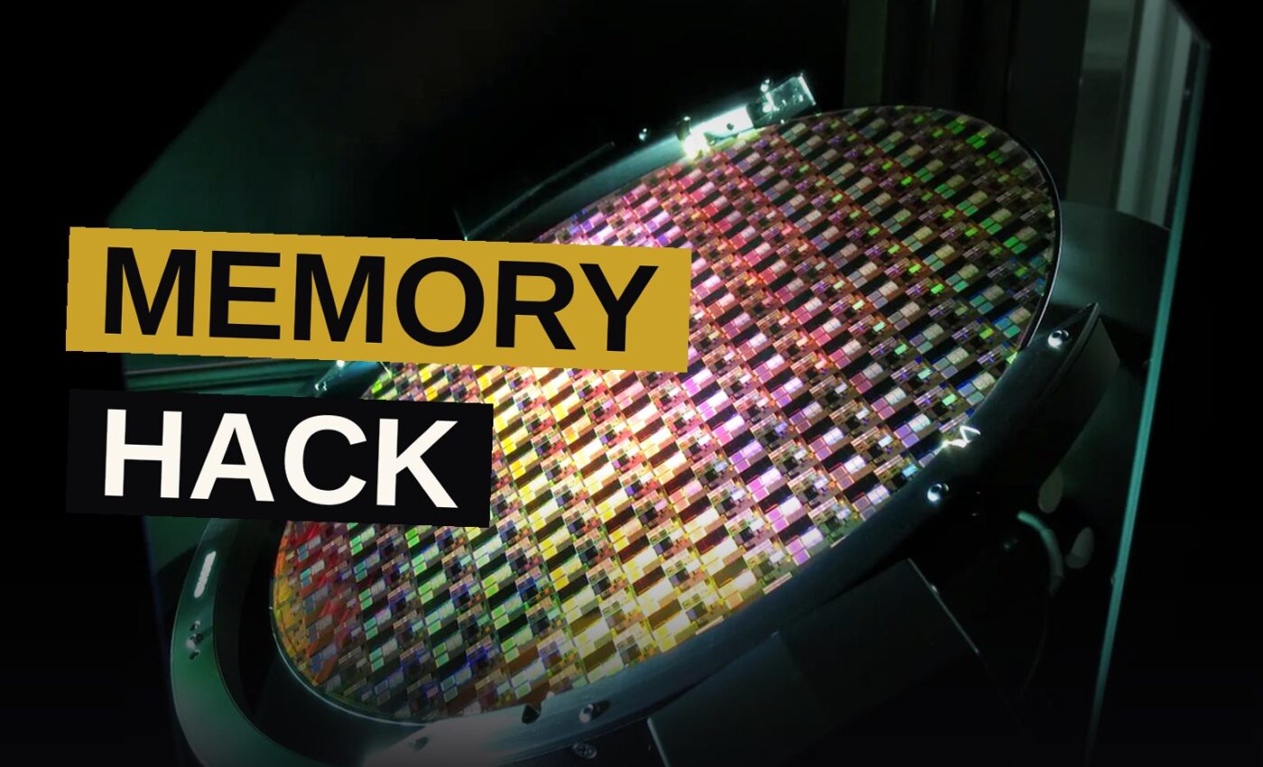
Kepler Computing, a San Jose, California-based startup founded in 2018, has come out of stealth mode with a claim: its new memory-chip architecture can ease the global shortage. The company says it can build high-bandwidth memory (HBM) and cache memory without the expensive extreme ultraviolet lithography (EUV) that chipmakers usually rely on.
Kepler says its “3D stacking” approach and a proprietary new material let it pack more memory into the same space. It says existing semiconductor factories can produce its chips with minimal retooling.
Funding and Fabs
Kepler has raised $468 million from backers including GlobalFoundries, Intel Capital, AMD Ventures, Baillie Gifford, and Bill Gates through his Gates Frontier fund. In July, the US Department of Commerce committed up to $245 million to Kepler for “develop in the US a new class of high-performance AI memory technology.”
Much of Kepler’s testing happens in Singapore, where GlobalFoundries—a manufacturing partner and $50 million investor—has a facility. Kepler has built “mini fabs” there over the past two years, working with GlobalFoundries’ 28-nanometer chips. It has also run tests in Burlington, Vermont.
The company’s timing follows a surge in demand for HBM, driven by AI workloads. SK Hynix and Micron are building multibillion-dollar fabs to meet that demand.
The Material Bet
Kepler’s pitch is that the market shouldn’t wait for new fabs. It says its approach works within existing ones.
“For a long time our thinking was that we’d work on SRAM first and then follow up with DRAM and HBM,” says Debo Olaosebikan, a Kepler cofounder and its chief executive officer. “But with the launch of ChatGPT [in 2022] and the explosion of demand for an HBM alternative, we started working on our HBM road map. Now we’re making SRAM and HBM in parallel.”
Kepler claims its SRAM matches the density of 2-nanometer or 3-nanometer chips without EUV. The company says it improved density using ferroelectrics, which read and write data at lower voltages. Sasi Manipatruni, a Kepler cofounder and its chief technology officer, says the team tried 35 material composites before settling on one.
“Once we found a way to solve the physics problem—as in the physical limitations for HBM—we came up with a material innovation that helps with the amount of memory you can have between chips,” he says.
Kepler says it converted a fab into a “next-generation” fab in eight months, versus a typical 24-month timeframe.
“Out goal is to take the fabs and architectures already built, and push them to the limits of physics,” Olaosebikan says.
“Kepler’s approach is at the sweet spot of our strategy.”
That’s Ed Kaste, senior vice president of GlobalFoundries’ CMOS business.
The bet is that retooling costs less than the $20 billion to $40 billion needed for new fabs. Whether Kepler can deliver at scale remains unproven.
Source: wired.com
Get the Notebook.
The day's best stories and every fresh verdict, in plain English, in your inbox by seven. One email a day, no more.